


ADALM 2000 Activity: CMOS Logic Circuits, Transmission Gate XOR
Objective
The objective of this lab activity is tore in force the basic principles of CMOS logic from the previous lab activity titled “Build CMOS Logic Functions Using CD4007 Array” and to gain additional experience with complex CMOS gates. Specifically, you will learn how to combine CMOS transmission gates and CMOS inverters to build transmission gate exclusive-OR (XOR) and XNOR logic functions.
Background
To construct the logic functions in this lab activity, you will be using the CD4007 CMOS array and discrete NMOS and PMOS transistors (ZVN2110 ANMOS and ZVP2110 APMOS)from the ADALP2000 analog parts kit .The CD4007 consists of three pairs of complementary MOSFETs, as shown in Figure 1. Each pair shares a common gate(pins 6, 3, and 10). The substrates of all PMOSFETs are common (positive supply Pin 14),as well as those of the NMOSFETs (ground Pin 7). For the left pair, the NMOS source terminal is tied to the NMOS substrate(Pin 7), and the PMOS source terminal is tied to the PMOS substrate (Pin 14). The other two pairs are more general-purpose. For the right pair, the drain terminal of the NMOS is tied to the drain terminal of the PMOS on Pin 12.
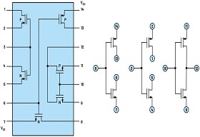
Figure 1. ACD4007 functional diagram.
The CD4007 is a versatile IC with many uses. For example, a single CD4007 can be used to make three inverters, an inverter plus two transmission gates, or other complex logic functions such as NAND and NOR gates. Inverters and transmission gates are particularly useful for building transmission gate XOR and XNOR logic functions. The schematic symbols for XOR and XNOR logic gates are shown in Figure 2.
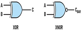
Figure 2. XOR and XNOR schematic symbols.
Static Discharge
The CD4007, like many CMOS integrated circuits, is easily damaged by static discharge. The CD4007 includes diodes to protect it from static discharge, but it can still be damaged if it is not handled carefully. Normally, one would use antistatic mats and wrist straps when working with static sensitive electronics. However, you may not have those when working at home outside a formal lab environment. A low budget way to avoid static discharge is to ground yourself before touching an IC. Discharging any built-up static charge before handling a CD4007 will help ensure that you do not have a broken chip halfway through the lab.
Materials
Directions
We will now combine the double-pole, single-throw (SPDT) transmission gates witch and two CMOS inverters to build an XOR gate(and XNOR)as shown in Figure 3. The two transmission gates work in tandem to realize a selector operation. Depending on the state of the A input, either Input B or the inverted version of Input B appears at the C (XOR) output. Two other inverters, M9 and M10, invert C to produce the CBAR(XNOR) output.
Build the XOR/XNOR circuit shown in Figure3 on your solder less breadboard. Use the CD4007 CMOS array for devices M1 to M6 and one ZVN2110 ANMOS and ZVP2110 APMOS for each of the two inverter stages: the M7 and M8 stage and the M9 and M10 stage. Use the fixed 5V power supply from the ADALM2000 to power your circuit.
There are two logic inputs A and B to the circuit. The non inverting XOR output is at Node C and an inverting version of the output is at Node C B A R to form the XNOR function.
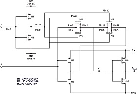
Figure 3. XOR and XNOR gate.
Hardware Setup
Configure both AWG outputs as DC sources for the first steps of the lab. The scope channels are to be used to monitor the inputs and outputs of the circuit as needed. The fixed +5V power supply is to be used to power your circuit. The fixed –5 V supply should be disabled during this lab.
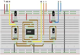
Figure 4.XOR and XNOR gate breadboard circuit.
Procedure
Connect Pin 6, which serves as the A input, to AWG1. Connect pins 1 and 9, which serve as the B input, to the output of AWG2.Connect pins 2, 5, and 12, which serve as the C output, to Scope Channel 1. Connect the drain terminals of M 9 and M 10,which serve as the CBAR output, to Scope Channel 2. Be sure to turn on the fixed 5V power supply.
First, apply logic low to A by opening the AWG control screen and setting AWG1 to 0 V DC. Apply logic low to the B input by setting AWG2 to 0 V DC.
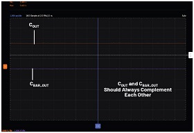
Figure 5.COUT and CBAR output.
Observe the C output of the gate on Scope Channel 1. A steady DC voltage should appear on the scope screen.
Now configure both AWG channels as square waves with 5V amplitude speak-to-peak and 2.5V off sets (0V to 5V swings). Set AWG1 to a frequency of 1kHz and AWG2 to a frequency of 2kHz or twice AWG1. Be sure to set the AWGs to run synchronously.
Observe both the C output and the CBAR output on the scope screen with respect to the signals at the A and B inputs.
Next, set AWG2 to the same 1 kHz frequency as AWG1 but set the phase of AWG2to 90°. Observe both the C output and the CBAR output on the scope screen with respect to the signals at the A and B inputs.
XOR Gate as a Phase Detector
A phase detector or phase comparator is a logic circuit that generates an analog output voltage signal, which represents the difference in phase between two logic signal inputs. It is a central element of a phase-locked loop (PLL). Detecting the phase relationship between signals is an important functional block in many systems, such as motor control, radar, telecommunication, demodulators, and servo mechanisms.
A phase detector for square wave signals can be made from an XOR logic gate. When the two signals being compared are completely in-phase—that is, phase difference is 0°—the XOR gate’s output will have a constant level of zero. When the two signals differ in phase by 10°, for example, the XOR gate’s output will be high for 10/180th or 1/18th of a cycle, the fraction of a cycle during which the two signals differ in value. When the signals differ by 180°, that is, one signal is high when the other is low, and vice versa, the XOR gate’s output remains high through out each cycle.
When an XOR gate phase detector is used in a PLL system, it generally locks near a 90° phase difference in the middle of the phase detection range. At 90°, the XOR has a 50% duty cycle square wave output at twice the frequency of the input. The square wave changes duty-cycle in proportion to the phase difference of the two input signals. Passing the output of the XOR gate through a low-pass filter results in an analog voltage that is proportional to the phase difference between the two signals. It requires inputs that are symmetrical square waves. If the duty cycle of one input is slightly different than the duty cycle of the other, the low-pass filtered output will have an offset from the ideal middle of the range at 90° of phase difference.
Directions
Add the RC low-pass filter shown in Figure 6 to your XOR breadboard circuit. Connect Scope Channel 1 to the output of the RC filter.
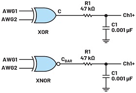
Figure 6. An XOR gate phase detector.
Hardware Setup
Configure both AWG channels as square waves with 5V amplitude speak-to-peak and 2.5 V offsets (0 V to 5 V swings). Set both AWG1 and AWG2 to a frequency of 1kHz. Also be sure to start with the phase of both AWG1 and AWG2 set to 0°.Be sure to set the AWGs to run synchronously.
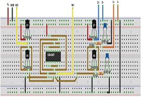
Figure 7.An XOR gate phase detector bread board circuit.
Procedure
Connect Scope Channel1 to the output of the RC filter at C1 to observe the filtered (DC) output of the phase detector. Connect Scope Channel2 to the output C of the XOR gate to observe the pulse width of the output of the logic gate.
AS copy plot example is presented in Figure 8.
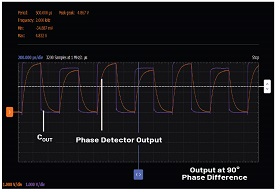
Figure 8. An XOR gate phase detector sample output.
Alternate Component Choices
The pair of inverters made using the four individual NMOS and PMOS transistors (ZVN2110 A and ZVP2110 A)could also be constructed from a second CD4007IC or CMOS inverters from a hex inverter IC such as a 74HC04 or CD4049. The CD4066 quad SPST switch could also serve as an alternative to the switches built from the CD4007.

The objective of this lab activity is tore in force the basic principles of CMOS logic from the previous lab activity titled “Build CMOS Logic Functions Using CD4007 Array” and to gain additional experience with complex CMOS gates. Specifically, you will learn how to combine CMOS transmission gates and CMOS inverters to build transmission gate exclusive-OR (XOR) and XNOR logic functions.
Background
To construct the logic functions in this lab activity, you will be using the CD4007 CMOS array and discrete NMOS and PMOS transistors (ZVN2110 ANMOS and ZVP2110 APMOS)from the ADALP2000 analog parts kit .The CD4007 consists of three pairs of complementary MOSFETs, as shown in Figure 1. Each pair shares a common gate(pins 6, 3, and 10). The substrates of all PMOSFETs are common (positive supply Pin 14),as well as those of the NMOSFETs (ground Pin 7). For the left pair, the NMOS source terminal is tied to the NMOS substrate(Pin 7), and the PMOS source terminal is tied to the PMOS substrate (Pin 14). The other two pairs are more general-purpose. For the right pair, the drain terminal of the NMOS is tied to the drain terminal of the PMOS on Pin 12.
Figure 1. ACD4007 functional diagram.
The CD4007 is a versatile IC with many uses. For example, a single CD4007 can be used to make three inverters, an inverter plus two transmission gates, or other complex logic functions such as NAND and NOR gates. Inverters and transmission gates are particularly useful for building transmission gate XOR and XNOR logic functions. The schematic symbols for XOR and XNOR logic gates are shown in Figure 2.
Figure 2. XOR and XNOR schematic symbols.
Static Discharge
The CD4007, like many CMOS integrated circuits, is easily damaged by static discharge. The CD4007 includes diodes to protect it from static discharge, but it can still be damaged if it is not handled carefully. Normally, one would use antistatic mats and wrist straps when working with static sensitive electronics. However, you may not have those when working at home outside a formal lab environment. A low budget way to avoid static discharge is to ground yourself before touching an IC. Discharging any built-up static charge before handling a CD4007 will help ensure that you do not have a broken chip halfway through the lab.
Materials
- ADALM2000 Active Learning Module
- Solder less bread board
- One CD4007 (CMOS array)
- Two ZVN2110 ANMOS transistors
- Two ZVP2110 APMOS transistors
Directions
We will now combine the double-pole, single-throw (SPDT) transmission gates witch and two CMOS inverters to build an XOR gate(and XNOR)as shown in Figure 3. The two transmission gates work in tandem to realize a selector operation. Depending on the state of the A input, either Input B or the inverted version of Input B appears at the C (XOR) output. Two other inverters, M9 and M10, invert C to produce the CBAR(XNOR) output.
Build the XOR/XNOR circuit shown in Figure3 on your solder less breadboard. Use the CD4007 CMOS array for devices M1 to M6 and one ZVN2110 ANMOS and ZVP2110 APMOS for each of the two inverter stages: the M7 and M8 stage and the M9 and M10 stage. Use the fixed 5V power supply from the ADALM2000 to power your circuit.
There are two logic inputs A and B to the circuit. The non inverting XOR output is at Node C and an inverting version of the output is at Node C B A R to form the XNOR function.
Figure 3. XOR and XNOR gate.
Hardware Setup
Configure both AWG outputs as DC sources for the first steps of the lab. The scope channels are to be used to monitor the inputs and outputs of the circuit as needed. The fixed +5V power supply is to be used to power your circuit. The fixed –5 V supply should be disabled during this lab.
Figure 4.XOR and XNOR gate breadboard circuit.
Procedure
Connect Pin 6, which serves as the A input, to AWG1. Connect pins 1 and 9, which serve as the B input, to the output of AWG2.Connect pins 2, 5, and 12, which serve as the C output, to Scope Channel 1. Connect the drain terminals of M 9 and M 10,which serve as the CBAR output, to Scope Channel 2. Be sure to turn on the fixed 5V power supply.
First, apply logic low to A by opening the AWG control screen and setting AWG1 to 0 V DC. Apply logic low to the B input by setting AWG2 to 0 V DC.
Figure 5.COUT and CBAR output.
Observe the C output of the gate on Scope Channel 1. A steady DC voltage should appear on the scope screen.
Now configure both AWG channels as square waves with 5V amplitude speak-to-peak and 2.5V off sets (0V to 5V swings). Set AWG1 to a frequency of 1kHz and AWG2 to a frequency of 2kHz or twice AWG1. Be sure to set the AWGs to run synchronously.
Observe both the C output and the CBAR output on the scope screen with respect to the signals at the A and B inputs.
Next, set AWG2 to the same 1 kHz frequency as AWG1 but set the phase of AWG2to 90°. Observe both the C output and the CBAR output on the scope screen with respect to the signals at the A and B inputs.
XOR Gate as a Phase Detector
A phase detector or phase comparator is a logic circuit that generates an analog output voltage signal, which represents the difference in phase between two logic signal inputs. It is a central element of a phase-locked loop (PLL). Detecting the phase relationship between signals is an important functional block in many systems, such as motor control, radar, telecommunication, demodulators, and servo mechanisms.
A phase detector for square wave signals can be made from an XOR logic gate. When the two signals being compared are completely in-phase—that is, phase difference is 0°—the XOR gate’s output will have a constant level of zero. When the two signals differ in phase by 10°, for example, the XOR gate’s output will be high for 10/180th or 1/18th of a cycle, the fraction of a cycle during which the two signals differ in value. When the signals differ by 180°, that is, one signal is high when the other is low, and vice versa, the XOR gate’s output remains high through out each cycle.
When an XOR gate phase detector is used in a PLL system, it generally locks near a 90° phase difference in the middle of the phase detection range. At 90°, the XOR has a 50% duty cycle square wave output at twice the frequency of the input. The square wave changes duty-cycle in proportion to the phase difference of the two input signals. Passing the output of the XOR gate through a low-pass filter results in an analog voltage that is proportional to the phase difference between the two signals. It requires inputs that are symmetrical square waves. If the duty cycle of one input is slightly different than the duty cycle of the other, the low-pass filtered output will have an offset from the ideal middle of the range at 90° of phase difference.
Directions
Add the RC low-pass filter shown in Figure 6 to your XOR breadboard circuit. Connect Scope Channel 1 to the output of the RC filter.
Figure 6. An XOR gate phase detector.
Hardware Setup
Configure both AWG channels as square waves with 5V amplitude speak-to-peak and 2.5 V offsets (0 V to 5 V swings). Set both AWG1 and AWG2 to a frequency of 1kHz. Also be sure to start with the phase of both AWG1 and AWG2 set to 0°.Be sure to set the AWGs to run synchronously.
Figure 7.An XOR gate phase detector bread board circuit.
Procedure
Connect Scope Channel1 to the output of the RC filter at C1 to observe the filtered (DC) output of the phase detector. Connect Scope Channel2 to the output C of the XOR gate to observe the pulse width of the output of the logic gate.
AS copy plot example is presented in Figure 8.
Figure 8. An XOR gate phase detector sample output.
Alternate Component Choices
The pair of inverters made using the four individual NMOS and PMOS transistors (ZVN2110 A and ZVP2110 A)could also be constructed from a second CD4007IC or CMOS inverters from a hex inverter IC such as a 74HC04 or CD4049. The CD4066 quad SPST switch could also serve as an alternative to the switches built from the CD4007.

.jpg "Hima Mal: Guiding Students Through Self Discovery & Beyond")


